- | Home |
- Company |
- Contact |
- News |
- S/ware Eng |
- Standards |
- Academic Support |
- Documents |

- | Requirements |
- Validation |
- RTOS |
- Analysis |
- Software |
- Resources |
- Products |
Segger J-Link Pro
Phaedsys has now closed |

J-Link ARM Pro is a refined version of the regular J-Link. It has an Ethernet interface in addition to the USB interface, as well as two additional LEDs which are used as hardware status indicators. When J-Link ARM Pro is used via USB it can be USB powered; for Ethernet use it is powered via the USB connector using a USB hub or the power supply that comes with it.
Furthermore J-Link ARM Pro comes with licenses for all J-Link related SEGGER software products: FlashDL, FlashBP, RDI, J-Flash, GDB Server, providing the optimum debugging solution for professional developers. J-Link ARM Pro can be used with almost all ARM debuggers, enabling download to flash memory with an unlimited number of breakpoints when debugging programs located in flash memory of most popular ARM microcontrollers. It also comes with the license to use J-Flash, SEGGER´s popular flash programming software.
J-Link ARM Pro is fully compatible with J-Link ARM and can be used "out-of- the-box". J-Link ARM Pro uses DHCP per default. The built-in webserver makes manual configuration easy and convenient.
All ARM7/9/11 and Cortex-M3 devices are supported; Cortex-M3 devices can be accessed via JTAG or SWD/SWO at high speed. The latest version of the J-Link software can be downloaded free of charge please contact us .
Features:
Fully compatible to J-Link ARM
Ethernet interface
USB 2.0 interface
Any ARM®7/9/11, Cortex™-M3 core supported, including thumb mode
More memory for future firmware extensions (ARM11, X-Scale, Cortex R4, Cortex A8)
Additional LEDs for power and RESET indication
Comes with web interface for easy TCP/IP configuration (built-in webserver)
Built-in GDB Server (planned to be implemented in the near future)
Serial Wire Debug (SWD) supported
Serial Wire Viewer (SWV) supported
Automatic core recognition
Maximum JTAG speed 12 MHz
Download speed up to 720 Kbytes/second * (higher download speeds will be available in the near future)
DCC speed up to 800 Kbytes/second *
Seamless integration into the IAR Embedded Workbench® IDE
Powered through USB or power supply which comes with J-Link ARM Pro
Support for adaptive clocking
All JTAG signals can be monitored, target voltage can be measured
Support for multiple devices
Fully plug and play compatible
Standard 20-pin JTAG connector
Wide target voltage range: 1.2V - 3.3V, 5V tolerant
USB and 20-pin ribbon cable included
Memory viewer (J-Mem) included
Comes with licenses for: J-Link ARM RDI, J-Link ARM FlashBP, J-Link ARM FlashDL, J-Link ARM GDB Server, J-Flash ARM
Software Developer Kit (SDK) available
Embedded Trace Buffer (ETB) support
Adapter for 5V JTAG targets available
14-pin JTAG adapter available
Galvanic isolation from host system via Ethernet
Optical isolation adapter available
Target power supply: J-Link can supply up to 300 mA to target with overload protection.
* = Measured with J-Link ARM Pro Rev. 1, ARM7 @ 50 MHz, 12MHz JTAG speed
Licencing
J-Link ARM Pro comes with licenses for all J-Link related SEGGER software products: J-Link ARM FlashDL, J-Link ARM FlashBP, J-Link ARM RDI, J-Flash ARM, J-Link ARM GDB Server, providing the optimum debugging solution for professional developers. J-Link ARM Pro can be used with almost all ARM debuggers, enabling download to flash memory with an unlimited number of breakpoints when debugging programs located in flash memory of most popular ARM microcontrollers. It also comes with the license to use J-Flash ARM, SEGGER´s popular flash programming software.
Available software packages
J-Link ARM FlashDL J-Link software, supporting download into flash memory
J-Link ARM FlashBP J-Link software supporting software breakpoints in flash
J-Link ARM RDI RDI software for J-Link. Allows using J-Link with any RDI compliant debugger
.
J-Flash ARM SEGGER's popular flash programming software for ARM cores.
J-Link ARM GDB Server Translates the GDB monitor commands into J-Link commands. Allows using J-Link with GDB (GNU Debugger).
J-Link SDK makes the entire functionality of J-Link available thru the exported API functions
Flash SDK An enhanced version of the JLinkARM.dll, which contains additional API functions for Flash programming.
Why PRO?
There are many aspects which make the J-Link Pro very attractive to use:
Price: Buying a J-Link ARM Pro, which comes with licenses for all J-Link-related SEGGER software, will save you a lot of money because buying a J-Link ARM and all licenses separate is more expensive.
Speed: J-Link Pro via TCP/IP provides higher download speed than J-Link via USB.
Usability: J-Link Pro can be used "out-of-the-box". A built-in J-Link ARM GDB Server is planned to be implemented in the near future.
Flexibility: Due to the Ethernet interface, long distances between the development PC and the target system are possible. You can set a default gateway for J-Link Pro, so it is also possible to use it in large intranets.
Security: When using J-Link ARM Pro via Ethernet, galvanic isolation of the development PC and the target system is supported.
Ready future use: J-Link ARM Pro provides more memory for future firmware extensions (e.g. ARM11, X-Scale, Cortex R4 and Cortex A8).
J-Link ARM Pro download speed
The following table lists J-Link ARM performance values (Kbytes/s) for writing to memory (RAM):
Revision |
ARM7 |
ARM9 |
J-Link ARM Pro Rev. 1 |
720.0 Kbytes/s |
|
Please note that the actual speed depends on various factors, such as JTAG, clock speed, host CPU core etc.
Built in Web Server
J-Link ARM Pro comes with a web server, which provides an easy-to-use web interface to configure J-Link Pro. It is possible to configure J-Link Pro for Ethernet via DHCP or manually. When configuring J-Link Pro manually it is also possible to set a default gateway which allows using J-Link Pro in large intranets without using DHCP. This enables you to configure J-Link ARM Pro without additional tools, just with a simple web browser
The web server also shows emulator information about the connected J-Link ARM Pro (serial number, firmware version) as well as the network configuration of the connected J-Link ARM Pro unit.
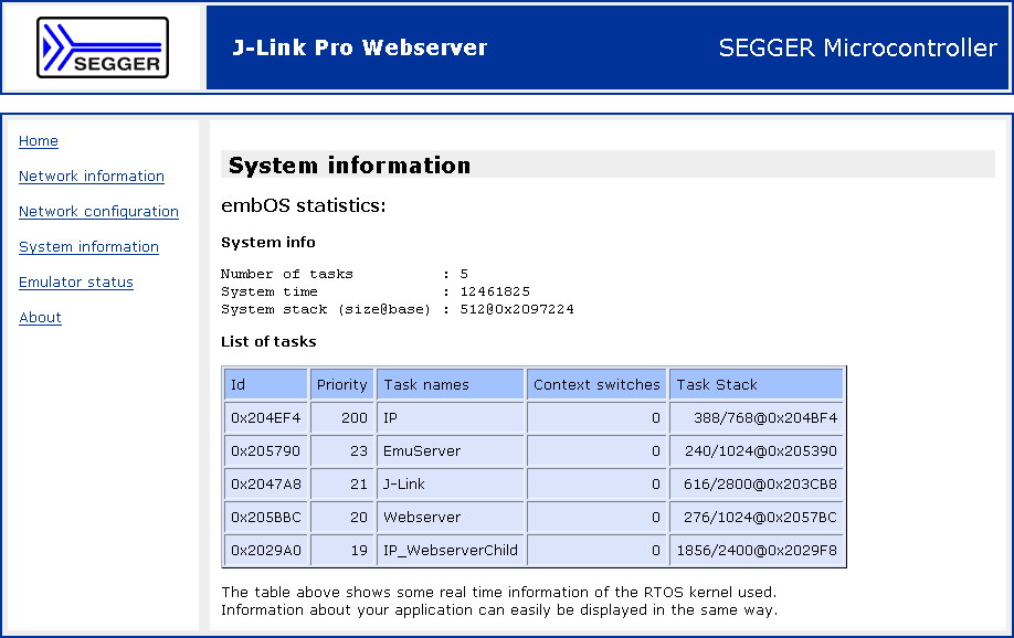
Moreover, the web server shows system information about the J-Link ARM Pro, such as the number of tasks which are currently running on the J-Link ARM Pro.

JTAG interface connection (20 pin)
There is a standard 20 pin connector defined by ARM. J-Link ARM has a built-in 20-pin JTAG connector, which is compatible with this standard.JTAG interface connector signals :
Pin |
Signal |
Type |
Description |
1 |
VTref |
Input |
This is the target reference voltage. |
2 |
Vsupply |
NC |
This pin is not connected in J-Link. |
3 |
nTRST |
Output |
JTAG Reset. Output from J-Link to the Reset signal of the target JTAG port. Typically connected to nTRST of the target CPU. This pin is normally pulled HIGH on the target to avoid unin- tentional resets when there is no connection |
5 |
TDI |
Output |
JTAG data input of target CPU. |
7 |
TMS |
Output |
JTAG mode set input of target CPU. |
9 |
TCK |
Output |
JTAG clock signal to target CPU. |
11 |
RTCK |
Input |
Return test clock signal from the target. |
| 13 |
TDO |
Input |
JTAG data output from target CPU. |
15 |
RESET |
I/O |
Target CPU reset signal. |
17 |
DBGRQ |
NC |
This pin is not connected in J-Link. |
19 |
5V-Target supply |
Output |
This pin can be used to supply power to the target hardware |
.Notes
All pins marked NC are not connected inside J-Link. Any signal can be applied here; J-Link will simply ignore such a signal.
Pins 4, 6, 8, 10, 12, 14, 16, 18, 20 are GND pins connected to GND in J-Link. They should also be connected to GND in the target system.
Pin 2 is not connected inside J-Link. A lot of targets have pin 1 and pin 2 connected. Some targets use pin 2 instead of pin 1 to supply VCC. These targets will not work with J-Link, unless Pin 1 and Pin 2 are connected on the target's JTAG connector.
Pin 3 (TRST) should be connected to target CPUs TRST pin (sometimes called NTRST). J-Link will also work if this pin is not connected, but you may experience some limitations when debugging. TRST should be separate from the CPU Reset (pin 15)
Pin 11 (RTCK) should be connected to RTCK if available, otherwise to GND.
Pin 19 (5V-Target supply) of the connector can be used to supply power to the target hardware. Supply volatage is 5V, max. current is 300mA. The output current is monitored and protected agains overload and short-circuit.
Power can be controlled via the J-Link commander. The following commands are available to control power:
.
SWD and SWO/SWV (also called SWV) compability
SWD overview
The J-Link and J-Trace support ARMs Serial Wire Debug (SWD). SWD replaces the 5-pin JTAG port with a clock (SWDCLK) and a single bi-directional data pin (SWDIO), providing all the normal JTAG debug and test functionality. SWDIO and SWCLK are overlaid on the TMS and TCK pins. In order to communicate with a SWD device, J-Link sends out data on SWDIO, syn- chronous to the SWCLK. With every rising edge of SWCLK, one bit of data is trans- mitted or received on the SWDIO. The data read from SWDIO can than be retrieved from the input buffer.
SWD connector pinout
The following table shows the SWD pinout
Pin |
Signal |
Type |
Description |
1 |
VTref |
Input |
This is the target reference voltage. It is used to check if the target has power, to create the logic-level reference for the input comparators and to control the output logic levels to the target. It is normally fed from Vdd of the target board and must not have a series resistor. |
2 |
Vsupply |
NC |
This pin is not connected in J-Link. It is reserved for compatibility with other equipment. Connect to Vdd or leave open in target system. |
3 |
Not used |
NC |
This pin is not used by J-Link. If the device may also be accessed via JTAG, this pin may be connected to nTRST, otherwise leave open. |
5 |
Not used |
NC |
This pin is not used by J-Link. If the device may also be accessed via JTAG, this pin may be connected to TDI, otherwise leave open. |
7 |
SWDIO |
I/O |
Single bi-directional data pin. |
9 |
SWCLK |
Output |
Clock signal to target CPU. It is recommended that this pin is pulled to a defined state of the target board. Typically connected to TCK of target CPU. |
11 |
Not used |
NC |
This pin is not used by J-Link. This pin is not used by J-Link when operating in SWD mode. If the device may also be accessed via JTAG, this pin may be connected to RTCK, otherwise leave open. |
13 |
SWO |
Output |
Serial Wire Output trace port. (Optional, not required for SWD communication.) |
15 |
RESET |
I/O |
Target CPU reset signal. Typically connected to the RESET pin of the target CPU, which is typically called "nRST", "nRESET" or "RESET". |
17 |
Not used |
NC |
This pin is not connected in J-Link. |
19 |
5V-Supply |
Output |
This pin is used to supply power to some eval boards. Not all JLinks supply power on this pin, only the KS (Kickstart) versions. Typically left open on target hardware. |
Pins 4, 6, 8, 10, 12, 14, 16, 18, 20 are GND pins connected to GND in J-Link. They should also be connected to GND in the target system
Serial Wire Output (SWO) overview
J-Link Pro can be used with devices that supports Serial Wire Output (SWO). Serial Wire Output (SWO) support means support for a single pin output signal from the core. It is currently tested with Cortex-M3 only.
Supported SWO speeds
J-Link Pro can handle up to 6MHz SWO speed.
Serial Wire Viewer (SWV) overview
The Instrumentation Trace Macrocell (ITM) and Serial Wire Output (SWO) can be used to form a Serial Wire Viewer (SWV). The Serial Wire Viewer provides a low cost method of obtaining information from inside the MCU. The SWO can output trace data in two output formats, but only one output mechanism is valid at any one time. The 2 defined encodings are UART and Manchester. The current J-Link implementation supports UART encoding only. Serial Wire Viewer uses the SWO pin to transmit different packets for different types of information. The three sources in the Cortex-M3 core which can output information via this pin are:
Instrumentation Trace Macrocell (ITM) for application-driven trace source that supports printf-style debugging. It supports 32 different channels, which allow it to be used for other purposes such as real-time kernel information as well.
Data Watchpoint and Trace (DWT) for real-time variable monitoring and PC-sampling, which can in turn be used to periodically output the PC or various CPU-internal counters, which can be used to obtain profiling information from the target.
Timestamping. Timestamps are emitted relative to packets.
Multiple devices in the scan chain
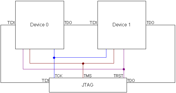
J-Link ARM can handle multiple devices in the scan chain. This applies to hardware where multiple chips are connected to the same JTAG connector. As can be seen in the drawing below, the TCK and TMS lines of all JTAG device are connected, while the TDI and TDO lines form a bus
Currently, up to 8 devices in the scan chain are supported. One or more of these devices can be ARM cores; the other devices can be of any other type but need to comply with the JTAG standard

Multi core debugging
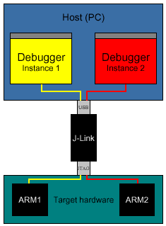
J-Link is able to debug multiple cores on one target system connected to the same scan chain.
How multi-core debugging works
Multi-core debugging requires multiple debuggers or multiple instances of the same debugger. Two or more debuggers can use the same J-Link / J-Trace simultaneously. Configuring a debugger to work with a core in a multi-core environment does not require special settings. All that is required is proper setup of the scan chain for each debugger. This enables J-Link / J-Trace to debug more than one core on a target at the same time.
|
 |
Phaedsys has now closed |


